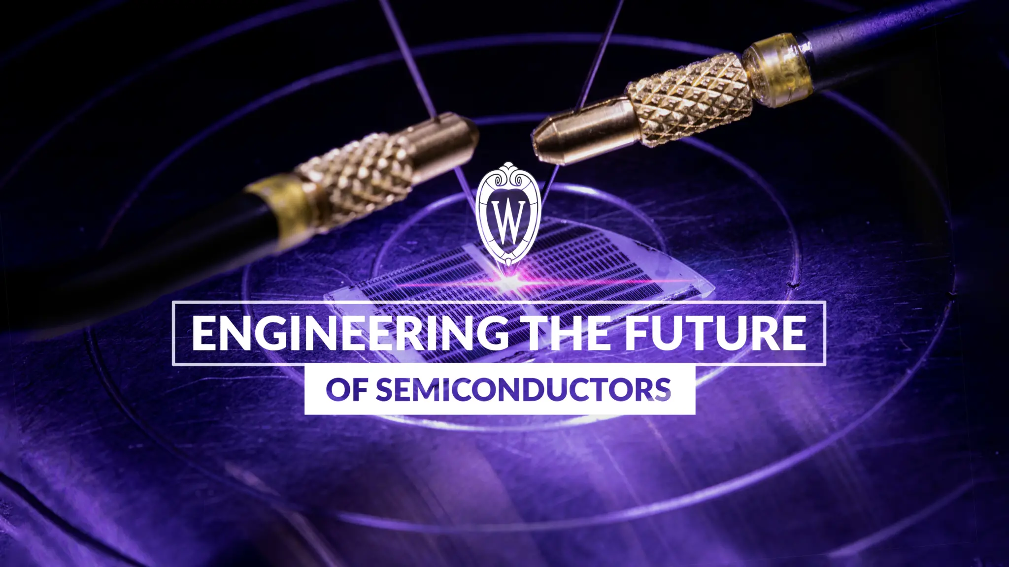
Semiconductors
Situated at the core of one of America’s elite research institutions, our college offers a rare environment for scientists who want to create the next generation of semiconducting materials.
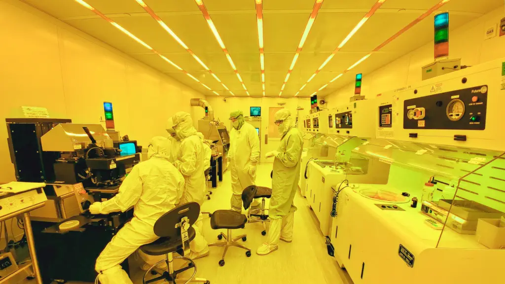

Research in action
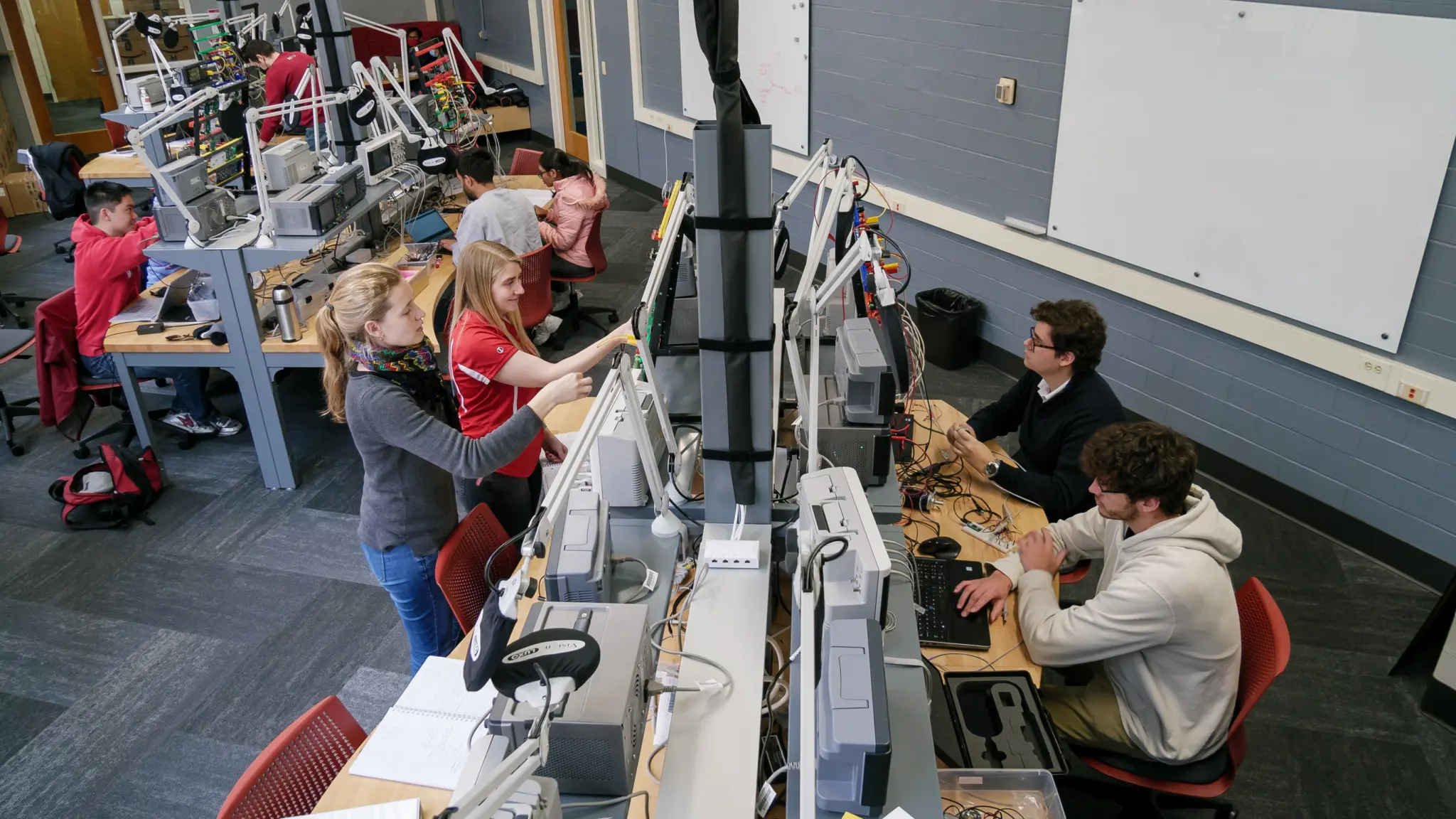
A large cohort of world-class researchers across our college is already working on areas vital to the future of the semiconductor industry.
Michael Arnold, the Beckwith Bascom Professor in materials science and engineering, is a world expert on carbon nanotubes, which are each about 1/10,000 the width of a human hair. Replacing silicon transistors on computer chips with these tiny tubes could boost the speed and efficiency of microchips five to 10 times.
“That’s a big deal, especially in mobile device computing and massive server farms that use tremendous amounts of electricity,” says Arnold, who has patented a process for attaching and aligning these tubes on silicon wafers and is already working with industry partners. “Energy-efficient computing is pretty important these days.”
So long, silicon
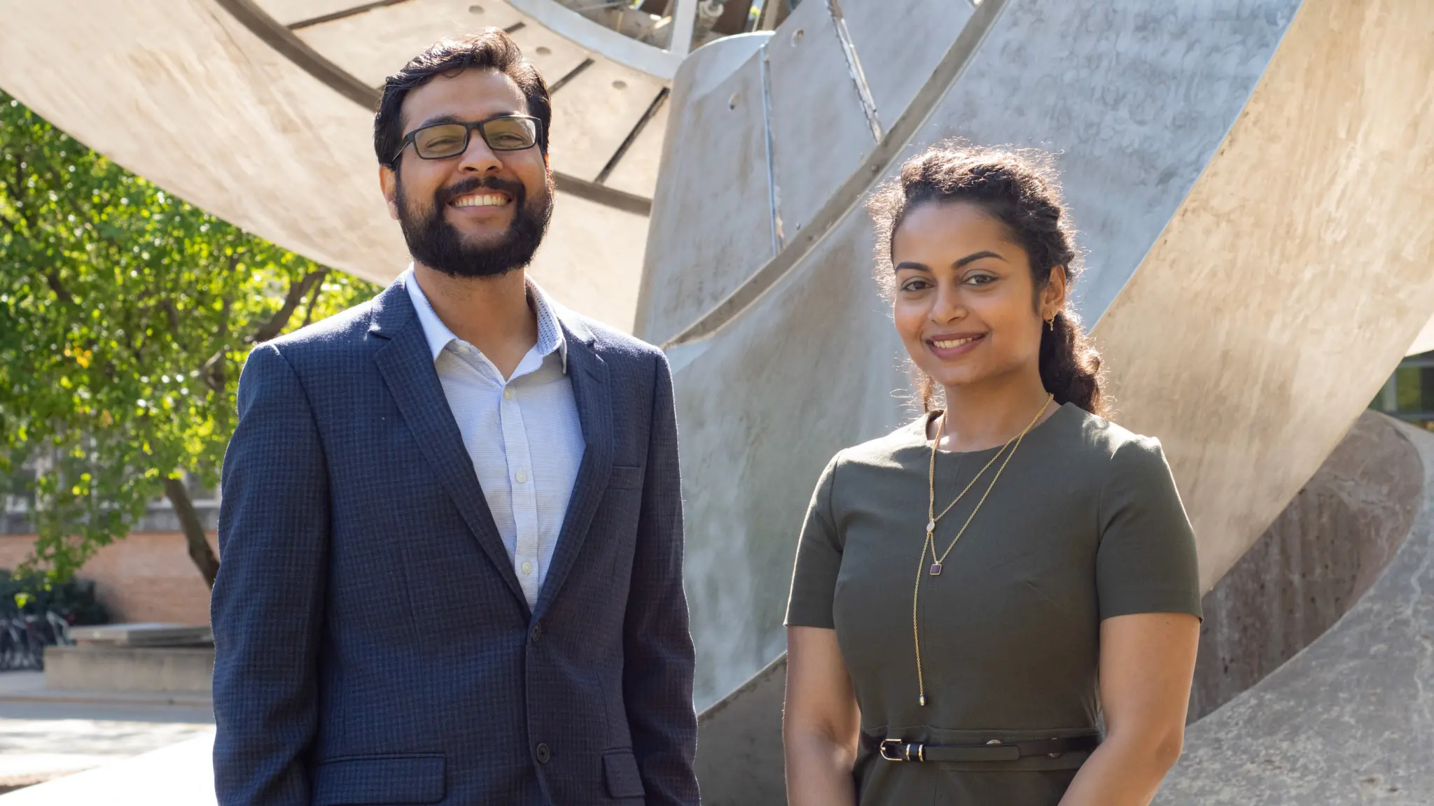
Other researchers are exploring classes of semiconductors that simply outperform silicon. Shubhra Pasayat and Chirag Gupta, assistant professors in electrical and computer engineering, are working with gallium nitride and gallium oxide, two semiconductors the industry is especially interested in. Their abilities to handle higher power than silicon makes them ideal for applications like ultrafast electric car chargers and more powerful components for 6G and 7G communications, as well as ultraviolet lasers, such as those Pasayat has developed.
Meanwhile, Zhenqiang “Jack” Ma, Lynn H. Matthias Professor and Vilas Distinguished Achievement Professor in electrical and computer engineering, is using diamonds and other materials to create state-of-the-art bipolar transistors.
Thinking thin
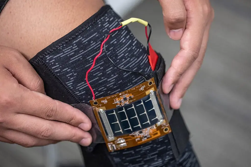
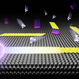
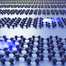
Many faculty are working on thin films and 2D materials, which are just one atom thick. When properly tuned or when layered with one another, these materials can be used as memory, sensors, solar cells and many other devices that currently rely on silicon. And because they are thin, they can be used in products like wearable devices, flexible displays and biosensors.
Fresh energy
Our college also has the talent to take advantage of the coming investment in next-gen semiconductors. Strategic hiring in the last few years has brought in new faculty with experience in semiconductor technology and manufacturing, including Pasayat, Gupta (a former engineer for the semiconductor device manufacturer Maxim Integrated) and Associate Professor Umit Yusuf Ogras, a former research scientist at Intel.
Other recent hires, such as Assistant Professors Daniel Rhodes, Ying Wang and Robert Jacobberger are exploring the potential of 2D materials.


Opportunity abounds
The effects of the COVID-19 pandemic and a long-simmering desire to rebuild technology manufacturing in the United States led to the country’s CHIPS and Science Act in August 2022, which provides billions of dollars for domestic semiconductor chip research and production.
Universities with advanced facilities, talented faculty, industry ties and a strong student body—like UW-Madison—are poised to lead the way. Already strong in semiconductor research and education, our college is ramping up those activities and leading a push to establish a semiconductor science center at UW-Madison.
Shaping future engineers
It’s not just faculty who will help drive the reenergized semiconductor industry—our students are already in high demand across the tech sector. According to Inside Higher Ed, the CHIPS Act will provide STEM-related higher education and workforce development at levels not seen since the era of the Space Race. That’s among the reasons we’re increasing our student body and pursuing partnerships with technical schools that can help lead more students to four-year or advanced degrees.
On the cusp of a domestic semiconductor revival, we’re engineering the future of an electronic essential.