February 26
@
4:00 PM
–
5:00 PM
Seamless Monolithic 3D Heterogeneous Integration Enabled by Advanced Epitaxy
Abstract: Three-dimensional heterogeneous integration (3D heterointegration) is emerging as the leading approach to enhancing performance in the field of microelectronics. However, this method often relies on complex wafer-to-wafer bonding processes, which introduce alignment challenges and interfacial defects. Alternatively, heteroepitaxy offers another route for implementing 3D heterointegration but suffers from material degradation due to defects and strain caused by lattice and thermal mismatches.
In this talk, I will introduce three new epitaxy paradigms designed to address the key limitations of current 3D heterointegration processes. First, I will discuss Remote Epitaxy, which enables wafer-scale exfoliation of ultra-thin membranes across a broad range of materials. By leveraging a 2D interlayer, these membranes can be transferred and monolithically 3D (M3D) integrated onto arbitrary substrates with ultra-high throughput and low cost, effectively addressing the challenges associated with wafer-to-wafer bonding. I will then present 2D-Assisted Heteroepitaxy, a technique that significantly reduces and, in some cases, eliminates defects in heteroepitaxy through strain relaxation mechanism at the 2D/3D interface. This advancement enhances materials quality and device performance over conventional heteroepitaxy, broadening opportunities for M3D heterointegration. Lastly, I will introduce single-crystal materials growth on amorphous substrates, which is made possible with a bold substrate design and carefully engineered materials growth conditions, offering an entirely new scheme of M3D heterointegration.
Building on these epitaxy paradigms, I will demonstrate various novel (opto)electronic devices as examples of their applications, including fabrication of world’s smallest micro-LED pixels (based on Remote Epitaxy), defect-free direct growth of III-V on silicon for next-generation optoelectronic applications (based on 2D-Assisted Heteroepitaxy), and advanced 3D stacking of 2D transistors (based on single-crystal materials growth on amorphous substrates). I will conclude the talk with a perspective on future materials development that could enable innovations across advanced 3D logic/memory, XR, energy, and quantum information, driven by new devices built upon advances in M3D heterointegration.
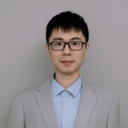
 Dr. Kuangye Lu
Bio: Dr. Kuangye Lu is currently a Postdoctoral Associate at the Research Laboratory of Electronics, Massachusetts Institute of Technology (MIT). He earned his Ph.D. in Mechanical Engineering from MIT in 2023 under the supervision of Prof. Jeehwan Kim, and earned a B.S. with honors in Physics from Zhejiang University (ZJU) in 2018.
His research focuses on the invention and development of advanced epitaxy techniques for compound semiconductors and 2D materials, as well as their heterointegration for device fabrication and applications. These efforts include the monolithic 3D integration of high-quality III-V optoelectronic devices on silicon, reconfigurable AI chips, and transistors engineered for next-generation advanced nodes.
Dr. Lu has authored peer-reviewed articles in high-impact journals, including Nature, Nature Nanotechnology, and Nature Electronics. He is the recipient of the Chu Ko-Chen Scholarship, the highest honor for graduates of ZJU, and the MIT Shangzhi Wu Fellowship. Additionally, Dr. Lu has served as a conference organizer of Advanced Epitaxy of Freestanding Membranes and 2D Materials (AEFM) Conference and a Review Editor for Frontiers in Energy Research. He also serves as a reviewer for journals including Nature Chemical Engineering, Science Advances, and Nano Letters.