September 14, 2023
@
4:00 PM
–
5:00 PM
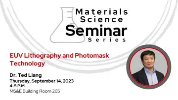
Materials Science Seminar Series presents Dr. Ted Liang on Thursday, September 14, from 4 to 5 p.m. The seminar is hosted by Professor Jason Kawasaki and will be held in MS&E building room 265. Dr. Ted Liang will be discussing EUV Lithography and Photomask Technology.
Abstract
Extreme ultraviolet lithography (EUVL) is a transformative technology used for high-volume manufacturing (HVM) of the world’s most advanced semiconductor devices. Operating at a wavelength of 13.5nm, EUVL overcomes the resolution limits of traditional optical lithography techniques and enables the patterning of ever smaller features for the fabrication of devices in the sub-10nm technology nodes. Due to the unique properties of EUV light (for example, it is absorbed by nearly all materials except He and H2), EUVL requires the use of reflective optics, complex masks (materials, manufacturing, and expensive infrastructure), stringent requirements for molecular cleanliness and precise control. This seminar highlights the key challenges and breakthroughs in EUVL development over the last 30 years and delves into several specific examples in EUV light source and mask technologies that illustrate the contributions from diverse MS&E disciplines to fundamental research and ultimately the engineering marvels producing leading-edge chips today. The following topics will be presented at a level suitable to provide an opportunity for a general audience to gain insights into the exciting field of EUV lithography and mask technology.
- Semiconductors from technology development to HVM and Moore’s law
- Overview of EUVL system and process: scanner, photomask, and photoresist
- Enabling technologies: EUV light from laser produced plasma, mirrors with atomically engineered Mo-Si multilayers
- The importance of photomask technology: materials, fabrication, and infrastructure
- Disruptive technology from concept to production: electron induced chemical etching and deposition for mask repair
- Engineering marvels: Pellicle with nanometer thick of large free-standing membranes including CNTs
- Collaborations among academia and industry from fundamental understanding to problem solving
Bio
Ted Liang is a Principal Engineer at Intel Corporation. After receiving his PhD in 1994 from the Materials Science Program at UW-Madison, he worked for 2 years in the Photon Physics group at NIST and then Intel as a Senior Lithography Engineer in 1996. He developed and transferred the lithography and metrology modules for flip chip bumping process in 1998 for Intel’s high-volume manufacturing (HVM). Since 2000, Ted has focused on Extreme ultraviolet (EUV) lithography and photomask technologies across research, pathfinding, and development and transfer to HVM. Ted has been instrumental in introducing many enabling technologies to the industry in areas of mask materials, metrology inspection, and repair. For his technology innovation and leadership, Ted has received two Intel Achievement Awards, the company’s highest recognition: once in 2006 for the development of a world-leading e-beam process technology from concept to production and again in 2021 for the development of industry first EUV actinic inspection system.
Ted has sponsored academic research and mentored graduate students at more than a dozen universities and national labs. He has been active in international conferences as invited speaker, panelist, program committee member, and conference chair. He has authored or co-authored more than 60 technical publications and has been awarded six U.S. patents. Outside of Intel, Ted enjoys visiting his two kids, spending time in the outdoors with his wife and golden retriever Madi (named after Madison).
 Materials Science Seminar Series – Speaker Dr. Ted Liang