October 16, 2025
@
1:00 PM
–
2:00 PM
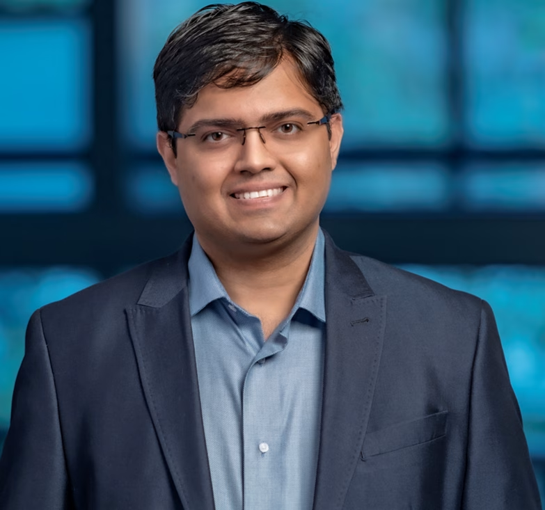
UW-Madison Department of Materials Science and Engineering welcomes Associate Professor Deep Jariwala. Their seminar, “Turbo-charging silicon: Do we have the materials and devices?”, will take place on Thursday, October 16 from 1 p.m. to 2 p.m. in MSE 265.

Bio
Deep Jariwala is an Associate Professor and the Peter & Susanne Armstrong Distinguished Scholar in the Electrical and Systems Engineering as well as Materials Science and Engineering at the University of Pennsylvania (Penn). Deep completed his undergraduate degree in Metallurgical Engineering from the Indian Institute of Technology in Varanasi and his Ph.D. in Materials Science and Engineering at Northwestern University. Deep was a Resnick Prize Postdoctoral Fellow at Caltech before joining Penn to start his own research group. His research interests broadly lie at the intersection of new materials, surface science and solid-state devices for computing, opto-electronics and energy harvesting applications in addition to the development of correlated and functional imaging techniques. Deep’s research has been widely recognized with several awards from professional societies, funding bodies, industries as well as private foundations, the most notable ones being the Optica Adolph Lomb Medal, the Bell Labs Prize, the AVS Peter Mark Memorial Award, IEEE Photonics Society Young Investigator Award, IEEE Nanotechnology Council Young Investigator Award, IUPAP Early Career Scientist Prize in Semiconductors, the SPIE Early career achievement award and the Alfred P. Sloan Fellowship. He has published over 150 journal papers with more than 22000 citations and holds several patents. He serves as the Associate Editor for Nano Letters (ACS) and has been appointed as a Distinguished Lecturer for the IEEE Nanotechnology Council for 2025.
Website: jariwala.seas.upenn.edu
Email: dmj@seas.upenn.edu
Abstract
Silicon has been the dominant material for electronic computing for decades and very likely will stay dominant for the foreseeable future. However, it is well-known that Moore’s law and Dennard’s scaling that propelled Silicon into this dominant position are long dead. Therefore, a fervent search for (i) new semiconductors that could directly replace silicon or (ii) new architectures with novel materials/devices added onto silicon or (iii) new physics/state-variables or a combination of above has been the subject of much of the electronic materials and devices research of the past 2 decades. In short, there is a pressing need for complementing and supplementing Silicon to operate with greater energy efficiency, speed and handle greater amounts of data. This is further necessary since a completely novel and paradigm changing computing platform (e.g. all optical computing or quantum computing) remains out of reach for now.
The above is, however, not possible without fundamental innovation in new electronic materials and devices. Therefore, in this talk, I will try to make the case of how novel layered two-dimensional (2D) chalcogenide materials1 and three-dimensional (3D) nitride materials might present interesting avenues to overcome some of the limitations being faced by Silicon (as well as Silicon Carbide) hardware. I will start by briefly introducing our past work on integration of 2D chalcogenide semiconductors with silicon2 to realize low-power tunnelling field effect transistors. In particular, I will focus on In-Se based 2D semiconductors2 for this application and extend discussion on them to phase-pure, epitaxial thin-film growth over wafer scales,3 at temperatures low-enough to be compatible with back end of line (BEOL) processing in Silicon fabs.
I will then switch gears to discuss memory devices from 2D materials when integrated with emerging wurtzite structure ferroelectric nitride materials4 namely aluminium scandium nitride (AlScN). First, I will present on Ferroelectric Field Effect Transistors (FE-FETs) made from 2D materials when integrated with AlScN and make the case for 2D semiconductors in this application.5-9
Next, I will introduce our work on Ferroelectric Diode (FeD) devices also based on thin AlScN.10-11 In addition, I will also present how FeDs provide a unique advantage in compute-in-memory (CIM) architectures for efficient storage, search as well as hardware implementation of neural networks.12 Finally, IF time permits, I will present ongoing work and opportunities to extend the application of AlScN memory devices into extreme environments.13-16
I will end the talk with a broad perspective on the role of novel materials that could turbo-charge silicon, silicon carbide and other pervasive semiconductor technologies for electronic computing.
References:
(1) Song, S.; Rahaman, M.; Jariwala, D. ACS Nano 2024, 18, 10955–10978.
(2) Miao, J.; ….et al. Jariwala, D. Nature Electronics 2022, 5 (11), 744-751.
(3) Song, S.;… et al. Jariwala, D. Matter 2023, 6, 3483-3498.
(4) Kim, K.-H.;…. et al. Jariwala, D. Nature Nanotechnology 2023, 18 (5), 422-441.
(5) Liu, X.;… et al. Jariwala, D. Nano Letters 2021, 21 (9), 3753-3761.
(6) Kim, K.-H.;.. et al. Jariwala, D. Nature Nanotechnology 2023, 18, 1044–1050.
(7) Kim, K.-H.; .. et al. Jariwala, D. ACS Nano 2024, 18 (5), 4180-4188.
(8) Song, S.;… et al. Jariwala, D. ACS Nano 2025.
(9) Song, S.;…et al. Jariwala, D. Applied Physics Letters 2023, 123 (18).
(10) Liu, X.; et al. Jariwala, D. Applied Physics Letters 2021, 118 (20), 202901.
(11) Kim, K.-H.;et al. Jariwala, D. ACS Nano 2024, 18 (24), 15925-15934.
(12) Liu, X.; et al. Jariwala, D. Nano Letters 2022, 22 (18), 7690–7698.
(13) Pradhan, D. K.; et al. Jariwala, D. Nature Electronics 2024, 7 (5), 348-355.
(14) He, Y.; et al. Jariwala, D. Applied Physics Letters 2023, 123 (12).
(15) He, Y.; et al. Jariwala, D. Nano Letters 2025.
(16) Pradhan, D. K.; et al. Jariwala, D. Nature Reviews Materials 2024, 9 (11), 790-807.