It’s been about 140 years since humanity began harnessing the power of the electron, pumping streams of the charged subatomic particles to electric devices in homes and businesses around the world.
But electrons are more than just their very useful negative charge. They also have a quantum property called angular momentum, otherwise known as spin, that can be manipulated to point in different directions. Researchers are currently studying ways to manipulate spin as part of a relatively new field called spintronics, which has the potential to upend the world as much as those first few jolts of electricity did.
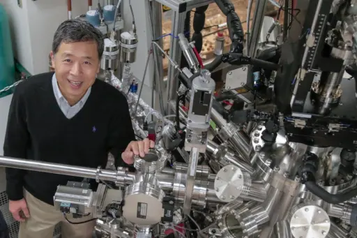 Chang-Beom Eom
The major promise of spintronics is the ability to use electron spin states (up or down) to control nanoscale transistors, much as electric current controls the conventional silicon transistors found in computer and memory chips. That could lead to new types of high-speed, low-power, high-density chips and solid-state memory devices.
There are still a few hurdles to overcome before the spintronics revolution gets underway. A breakthrough by University of Wisconsin-Madison researchers detailed in the journal Nature Communications is bringing widespread use of spintronics closer to reality.
Chang-beom Eom, a professor of materials science and engineering and physics at UW-Madison, and his collaborators have designed a new structure that leverages a little-studied class of materials called antiperovskites to manipulate spin states. The unique properties of the material creates non-colinear antiferromagnetism, which allows for the generation of previously-challenging directions of spin, and the motion of these spins into other layers of the structure.
In practical terms, the spin direction produced by the material means the structure accommodates three times the storage density of other spintronic devices with a much smaller power consumption. “This is an ideal way to make very-high-density, low-power spintronic devices,” says Eom. “We have created a very tiny system that controls the magnetization in ways not previously accessible.”
To create the device, the team developed methods to grow single crystal thin films composed of manganese-gallium-nitride (Mn3GaN) in which to create the spin motion. They then deposited a thin layer of a nickel/iron ferromagnetic alloy on top in which to transfer the angular momentum.
One reason this bilayer “heterostructure” device has such unique properties is because of the manganese-gallium-nitride’s antiperovskite crystal structure. Eom has expanded his studies of perovskite oxide crystal structures, which he has researched over the past few decades, into antiperovskites because the materials are very tunable and have many potential uses in electronics and other applications.
Researchers have attempted to create spintronic thin-film devices using other materials including platinum and heavy metals. “An additional advantage of this structure is that the manganese-gallium-nitride material is comprised of low cost and abundant elements,” says Eom.
That, plus the fact that the device manipulates spin states at room temperature, makes it even more practical.
The Army Research Office, an element of the U.S. Army Combat Capabilities Development Command’s Army Research Laboratory, which provides funding for the research, is also impressed by the advance. “Professor Eom’s work on controlling nano-magnets with electricity has important implications for the Army’s modernization efforts, which will rely on advances in low-power computing and fast magnetic memory,” says Evan Runnerstrom, program manager in materials design in the Army Research Office. “This unconventional but effective approach opens the door to efficient and fast spintronic devices for use in these demanding applications.”
Eom has applied for a patent on the device structure through the Wisconsin Alumni Research Foundation and is currently investigating other engineered antiperovskite devices. “The ability to manipulate spin structures and spin current has tremendous possibilities,” he says. “This is the first step in demonstrating how to do it.”
Eom is the Raymond R. Holton Chair Professor and Theodore H. Geballe Professor in materials science and engineering and physics at UW-Madison.
Tianxiang Nan, Camilo Quintela, Julian Irwin, Neil Campbell, Lu Guo and Mark Rzchowski of UW-Madison also contributed to the paper. Additional authors include G. Gurung, D.F. Shao and E.Y. Tsymbal of the University of Nebraska-Lincoln; J. Gibbons and D.C. Ralph of Cornell University; K. Song of KIMS, Changwon, South Korea; S.-Y. Choi of POSTECH, Pohang, South Korea; R.D. Johnson of Clarendon Laboratory, Oxford University and, with P. Manuel, University College London; R.V Chopdekar of Lawrence Berkeley National Laboratory; I. Hallsteinsen of Lawrence Berkeley National Laboratory and, with T. Tybell, 2the Norwegian University of Science and Technology, Trondheim, Norway; P.J. Ryan of Dublin City University and, with J.-W. Kim and Y. Choi, Argonne National Laboratory; and P.G. Radaelli of Clarendon Laboratory, Oxford University.
The team at UW-Madison acknowledges support by the National Science Foundation (NSF) under DMREF Grant DMR-1629270, the University of Wisconsin Materials Research Science and Engineering Center (DMR-1720415), the Army Research Office through Grant W911NF-17-1-0462 and AFOSR FA9550-15-1-0334, US Department of Energy (DOE), Office of Science, Office of Basic Energy Sciences under Award DE-FG02-06ER46327.