Using a revolutionary ultrafast camera, engineers at the University of Wisconsin-Madison have developed a new way to characterize organic glass thin films. This understanding could lead to new types of organic glass semiconductors. The research appears in the March 2023 issue of the journal NanoLetters.
 Paul Voyles
Glass may seem neat and orderly, but on the molecular level it’s quite messy; in fact, that’s one of the very definitions of glass. It’s a structurally disordered material (unlike a crystal, in which molecules are arranged in a rigid structure). “Think of glass as marbles in a jar, where the molecules are all jumbled up,” says Paul Voyles, a professor of materials science and engineering at the University of Wisconsin-Madison. “Crystals are more like eggs in an egg carton.”
That order gives crystals internal boundaries between grains that can interact with light or electrons. Glass, however, does not have these boundaries, meaning, for instance, light can travel through silica or window glass uninterrupted.
There’s a new glass in town, though: Recently, UW-Madison chemist Mark Ediger fabricated an organic glass from a phenanthroperylene ester using a technique called physical vapor deposition, in which the molecules are turned into a vapor and then condensed into a thin film. Some of the plate-shaped molecules in the new glass line up in neat columns, making it a glass with a little bit of order that could be used as a semiconductor that can transport electrons or emit light. That could be useful in producing cell phone displays, large monitors and organic photovoltaic cells.
After Ediger created the glass, the research team wanted to study the column lengths and controlling factors, their orientations and alignments.
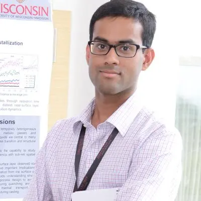
 Debaditya Chatterjee
These columns are extremely small, on the scale of 10 nanometers, and scanning transmission electron microscopy can use tiny beams of electrons to measure such miniscule materials. But it’s not possible to use the same process with this organic glass. “The disadvantage of electrons is they tend to turn organic materials into goo,” says Voyles. “They damage the materials quite quickly as we look at them. Part of our innovation was to study the structure of these materials very quickly, using a super-high-speed camera for electrons.”
The camera, which enables low-dose 4D scanning transmission electron microscopy (4D STEM), is one of the fastest in the world. Developed with a California-based company called Direct Electron Incorporated, it is housed in the UW-Madison Nanoscale Imaging and Analysis Center. The camera captures up to 87,000 images per second, allowing the researchers to keep the electron probe moving. “It lets us look fast enough that we’re looking at a singed piece of this material instead of one that’s burned to a crisp,” jokes Voyles.
The 4D STEM experiments were run and analyzed by Debaditya Chatterjee, who received his PhD in December 2022. The system generates data on the scale of multiple terabytes, so graduate student Shuoyuan Huang also developed software and algorithms to process all of that information.
Ultimately, the team could describe the length and orientation of the phenanthroperylene ester columns and provide some insight into how they formed.
For Voyles, the study was an important validation of using 4D STEM for studying organic glass, opening the door to new research directions. “These sorts of weird ‘edge cases’ push our understanding of the difference between glasses and crystals,” says Voyles. “This is one of the ways I think materials science advances. We make new stuff that doesn’t fit in any of the old categories or old theories. That’s how we push forward understanding of how materials work in the world, how we make them, and how they get their properties.”
Paul Voyles is Harvey D. Spangler Professor in materials science and engineering. In addition to Voyles, Ediger, Chatterjee and Huang, other UW-Madison authors include Kaichen Gu and Jianzhu Ju in the Department of Chemistry; and Junguang Yu and Professor Lian Yu in the School of Pharmacy. Harald Bock of the University of Bordeaux also contributed to the paper.
The authors acknowledge funding from UW-Madison MRSEC through National Science Foundation Award DMR-1720415.
Featured image caption: Graduate student Shuoyuan Huang works at the 4D STEM microscope in the basement of the UW-Madison Materials Science and Engineering building. The machine can capture up to 87,000 images per second. Credit: Joel Hallberg.