Using innovative semiconductor fabrication techniques, a team of University of Wisconsin-Madison electrical engineers has developed a new type of device that can convert heat directly into electricity.
The innovation—a near-field thermophotovoltaic device—could lead to new or more efficient energy sources. It could also enable the generation of electricity by harvesting waste heat from industrial processes like cement or steel production.
Led by Eric Tervo, an assistant professor of electrical and computer engineering and mechanical engineering at UW-Madison, the team includes colleagues at the National Renewable Energy Laboratory in Golden, Colorado. The researchers describe their “large-area, near-field thermophotovoltaics” in a paper published in the journal Advanced Materials on December 15, 2024.
“This device checks every single box—low-maintenance, high-power-density and scalability,” says Tervo. “You can use it with a huge variety of heat sources across a very large range of temperatures. It could be slotted into all sorts of energy systems, whether those are renewables or classic fossil fuel or nuclear systems. It opens up new technology and system options that you don’t have with these other types of heat engines.”
Much of today’s energy comes indirectly from heat: For example, coal, some natural gas power plants and nuclear reactors boil water, producing steam that spins electricity-producing turbines. But these processes are large, maintenance-heavy and centralized.
Thermophotovoltaics are simpler. They convert infrared radiation (a form of heat) directly into electricity similar to the way in which solar cells convert sunlight into electricity—no steam or turbines necessary.
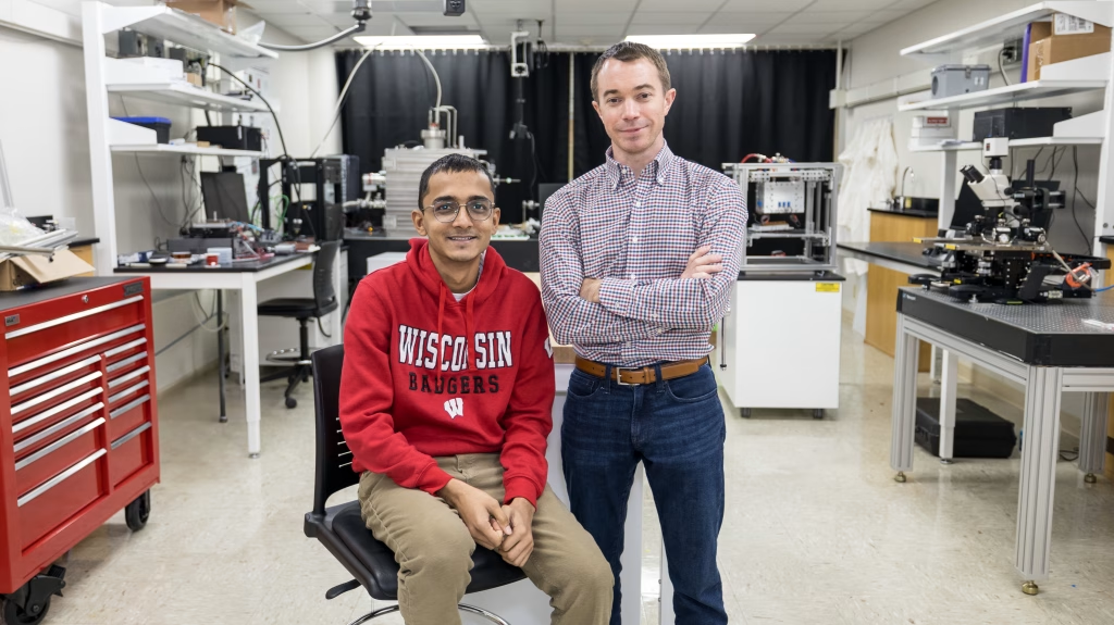
 ECE graduate student Parth Solanki (left) and Assistant Professor Eric Tervo. Photos by: Joel Hallberg
Current state-of-the-art thermophotovoltaics harvest what is called far-field infrared energy, which is emitted from all hot objects. These devices, however, are not very energy dense, meaning they have limited applications.
A more promising type of radiation called near-field infrared is more energy dense but can only be captured if the cell is extremely close to the hot object. Currently, harvesting this infrared energy is a difficult physics and engineering problem: Near-field devices require a nano-scale gap between their emitter layer, which collects heat and gives it off it as infrared radiation, and the thermophotovoltaic cell itself. When the “nanogap” is in place, light can transmit from the emitter to the cell as if the gap was not there at all, and the cell can efficiently convert the heat into electricity.
That’s why Tervo and his colleagues at the National Renewable Energy Laboratory pioneered a process to fabricate a precise nanogap. Using a material deposition technique called metalorganic vapor phase epitaxy, the team deposited a 150-nanometer layer of semiconductor material on the emitter, then etched away all but a grid of pillars. When the emitter is sandwiched on top of the thermophotovoltaic layer (which is made from a different semiconductor), the pillars ensured a consistent 150 nanometer nanogap across the entire structure.
Though the first devices they created are only 5 millimeter by 5 millimeter, about the width of a pencil, stacking the two layers with a 150 nm gap is the equivalent of putting two football fields on top of each other with a perfect 0.1 inch gap. “If any bending or tiny imperfection comes between the layers, it won’t work,” says Tervo.
Tests show the near-field thermophotovoltaic device works as predicted, producing 25 times more energy than the same cells set up to harvest far-field infrared energy.
Importantly, the fabrication technique is compatible with current semiconductor materials and fabrication technologies, making it easily scalable without major retooling or process changes.
Now that they have a proof of concept, Tervo and his colleagues next plan to scale the thermophotovoltaic devices up into the centimeter range and make them even thinner. They also plan to develop a silicon emitter to reduce future manufacturing costs.
“There are definitely still challenges to overcome,” says Tervo, who is optimistic that the device is on the path to future commercialization. “But you can remove layers. You can make the substrate thinner. You can make the gap smaller. And all this will get you to higher and higher power.”
Other UW-Madison authors include Parth Solanki. Other authors include Jennifer Selvidge, Ryan M. France, John Goldsmith and Myles A. Steiner of the National Renewable Energy Lab.
The authors acknowledge support from the National Renewable Energy Laboratory under DOE contract DE-AC36-08GO28308 and the Laboratory Directed Research and Development (LDRD) Program at NREL. Additional support was provided by the University of Wisconsin-Madison Office of the Vice Chancellor for Research and the Wisconsin Alumni Research Foundation.
Top image: UW-Madison ECE graduate student Parth Solanki is part of a team using precise semiconductor engineering techniques to create a nanogap between the emitter and thermophotovoltaic semiconductor in thermophotovoltaic cells, allowing them to harness energy from near-field infrared radiation. Photo by: Joel Hallberg.