University of Wisconsin-Madison engineers have discovered why defects form in 3D-printed high-end metal parts like titanium aluminide jet engine turbine blades.
They used a bespoke synchrotron X-ray imaging system to identify the phenomenon, which occurs in parts created with an up-and-coming additive manufacturing technology called electron beam melting.
Led by Lianyi Chen, an associate professor of mechanical engineering at UW-Madison, the researchers detailed their findings in a paper published April 7, 2026, in the journal Nature Communications.
Electron beam melting allows manufacturers to create complex metal parts that would be impossible or too costly to produce using other manufacturing methods. It’s an important technology for making high-end parts for aerospace, for example, or plasma-facing tungsten components for future fusion energy power plants.
However, metal parts created with the technology have defects—such as small voids inside the material—that significantly compromise the finished part’s reliability and durability. As a result, those 3D-printed parts can’t be used for critical applications where failure is not an option.
“We knew that defects form inside parts during the electron beam melting process, but we didn’t know why,” says Chen. “Industry adoption of electron beam melting has been growing rapidly in recent years, so it’s very important to understand the mechanism behind defect formation so we can figure out ways to avoid the defects.”
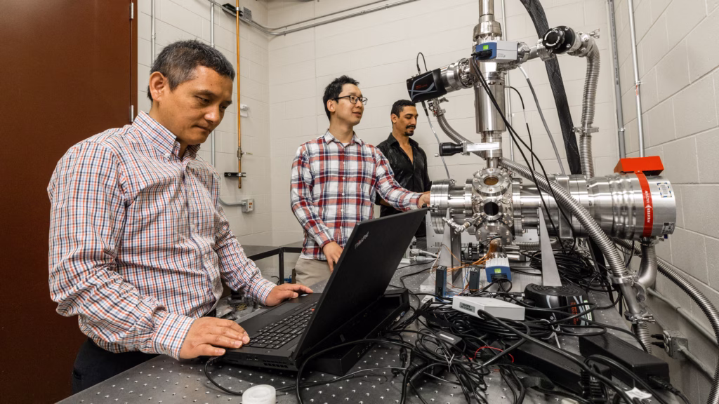 Associate Professor Lianyi Chen (left), graduate student Jiandong Yuan (center), and Luis Escano, early-career entrepreneur in residence in the college’s Grainger Institute for Engineering, work with the electron beam melting system in Chen’s lab. Credit: Joel Hallberg.
The technology relies on an electron beam to melt and fuse powdered metal together under a vacuum to build parts layer by layer. However, until 2022, when Chen and his collaborators developed the world’s first electron beam melting system for in-situ high-speed synchrotron X-ray imaging and diffraction to study the melting process in real time, researchers couldn’t observe what’s happening under the liquified powder, or liquid pool, and inside the part as it’s being printed.
Using their system, Chen and his team saw, in unprecedented detail, that the electron beam caused bubbles to form in the liquid right under the melt pool surface. As these bubbles exploded, they induced instabilities in the liquid pool that caused defects in the printed parts.
Jiandong Yuan, a graduate student in Chen’s group and first author on the paper, says these new insights into the printing process could help manufacturers improve electron beam melting technology. “Our work can also help researchers develop new criteria for material design as well as better computer models that take this bubble phenomenon into account, which could enable defect-free parts,” Yuan says.
Lianyi Chen is the Kuo K. & Cindy F. Wang Associate Professor in mechanical engineering.
UW-Madison co-authors on the paper include Luis Escano, Junye Huang, Ali Nabaa and Qingyuan Li. Additional co-authors include Samuel Clark and Kamel Fezzaa from Argonne National Laboratory.
This research was supported by the U.S. Department of Commerce (award number 70NANB21H039), and used resources of the Advanced Photon Source, a U.S. DOE Office of Science user facility operated for the DOE Office of Science by Argonne National Laboratory under contract number DE-AC02-06CH11357.
Featured image caption: Graduate student Jiandong Yuan (left) and Luis Escano, early-career entrepreneur in residence in the college’s Grainger Institute for Engineering, work with the electron beam melting system in Associate Professor Lianyi Chen’s lab. Credit: Joel Hallberg.