University of Wisconsin-Madison electrical engineers have dramatically improved a semiconductor-based imaging system that makes near-infrared light visible to the naked eye.
Near-infrared is the band of electromagnetic radiation between roughly 750 and 1,400 nanometers; it carries more information than visible light, making it useful in an array of applications, including noninvasive inspection of food, pharmaceuticals, plastics, textiles, semiconductors and other electronics. It is also used in bioimaging, agriculture, communications, machine vision, astronomy and night-vision technology.
The researchers’ system, which operates passively, or without the need for an external power source, could improve the efficiency and portability of near-infrared devices used for these and other emerging applications.
UW-Madison electrical and computer engineering PhD student Rabeeya Hamid led the research, along with Demeng Feng (PhDECE ’24) and Mikhail Kats, a professor of electrical and computer engineering. The team also included collaborators in Dan Congreve’s group at Stanford University and a scientist at Argonne National Lab. The researchers describe the nanoscale enhancements in a paper published in November 2025, in the journal Advanced Functional Materials.
While certain cameras can “see” near-infrared light, the un-aided human eye cannot. A converter must change the low-energy photons in the near-infrared range into the higher-energy photons of the visible range. Existing devices that do this typically require an external power source that helps boost the signal. Some passive systems do exist but can only detect very intense near-infrared radiation.
For many years, however, researchers have investigated an alternative model in which organic semiconductors use quantum processes to upconvert near-infrared to visible light. In this method, called triplet-triplet annihilation, the low-energy infrared photons interact with the semiconductor material, transferring their energy to two low-energy states, which then transfer their energy to a single high-energy state. This then emits a single high-energy photon in the visible spectrum that can be seen with the human eye or conventional cameras. Most importantly, no outside energy is needed to complete this conversion.
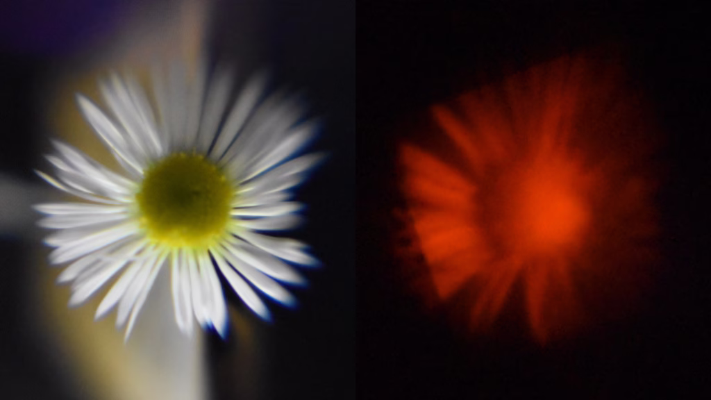 Nanoscale upgrades to the semiconductor imaging system improves up-conversion of near-infrared to visible light, allowing for better night vision and sensing. Submitted photo.
“The triplet-triplet annihilation process in solid-state films has been studied for at least a decade,” says Hamid. “But it’s one thing to convert photons from low energy to high energy, and another to actually use it for practical imaging. We spent several years trying to make this imaging a reality.”
Hamid, Kats, Feng and their collaborators hypothesized that, with some nanoscale modifications, they might be able to significantly boost the efficiency of the triplet-triplet annihilation process, and to build an optical system that can be positioned in front of the human eye.
The researchers designed two new nanophotonic components to enhance the absorption and collection of light in these semiconductors, which are made of extremely thin layers of two organic semiconductors called Y6 and rubrene, which were designed and synthesized by Pournima Narayanan and several other Stanford collaborators.
The first component they developed is a coating for the semiconductor that acts as a back-reflector, enhancing the amount of light the material is able to emit. The team applied alternating layers of the dielectric materials niobium pentoxide and silicon dioxide to the semiconductor. This thin coating, less than a micrometer thick, succeeded in boosting the emission power of the semiconductor 2.5 times.
The researchers also sought to increase the amount of near-infrared radiation the semiconductor material could absorb. To do this, they deposited the semiconductor material on top of a layer of tiny gold nanopillars, fabricated with the same methods used in microchip manufacturing. When illuminated by near-infrared light, the electrons in the pillars become excited in a process called plasmon resonance, which increases the absorption. In this case, the addition of the pillars doubled the absorption of near-infrared light at critical wavelengths.
When fabricated together on the semiconductor, these nanoscale enhancements quadrupled the image intensity produced by the imaging system, amplified low-intensity light orders of magnitude more than other emerging near-infrared technologies, and showed resolution levels on par with commercial systems that use external power sources within a section of the infrared spectrum. The researchers believe that, with additional enhancements, they could further boost the system’s sensitivity and extend its working wavelength range, making it viable for commercialization.
Kats says the team is eager to move forward. “I’m thrilled that we have been able to perform up-conversion imaging at low intensities, but the demonstration in this paper only goes out to a wavelength of 950 nanometers, missing a significant part of the near infrared,” he says. “We have solid ideas of how to perform passive imaging across much more of the infrared spectrum—at which point transition to an industrial partner or even a startup company becomes a possibility.”
Mikhail Kats is the Antoine-Bascom and Jack St. Clair Kilby Professor of electrical and computer engineering at the University of Wisconsin-Madison. Other UW-Madison authors include Justin S. Edwards, Minjeong Kim, Shenwei Yin, Sanket Deshpande and Chenghao Wan. Other authors include Pournima Narayanan, Manchen Hu, Emma Belliveau, Linda Pucurimay and Daniel N. Congreve of Stanford University and David A. Czaplewski of Argonne National Laboratory.
The UW-Madison authors acknowledge support from the Defense Advanced Research Projects Agency (DARPA) grant HR00112220010; the Center for Nanoscale Materials, a U.S. Department of Energy Office of Science User Facility, supported under Contract No. DE-AC02-06CH11357; and the UW-Madison Wisconsin Centers for Nanoscale Technology, partially supported by the NSF through the University of Wisconsin Materials Research Science and Engineering Center (DMR-2309000).
Top image caption: Using photonic engineering techniques, PhD student Rabeeya Hamid (center) enhanced an organic semiconductor’s ability to passively upconvert near-infrared signals into visible light. Credit: Submitted photo.